Sony Unveils World’s First Stacked CMOS with 2-Layer Transistor Pixels
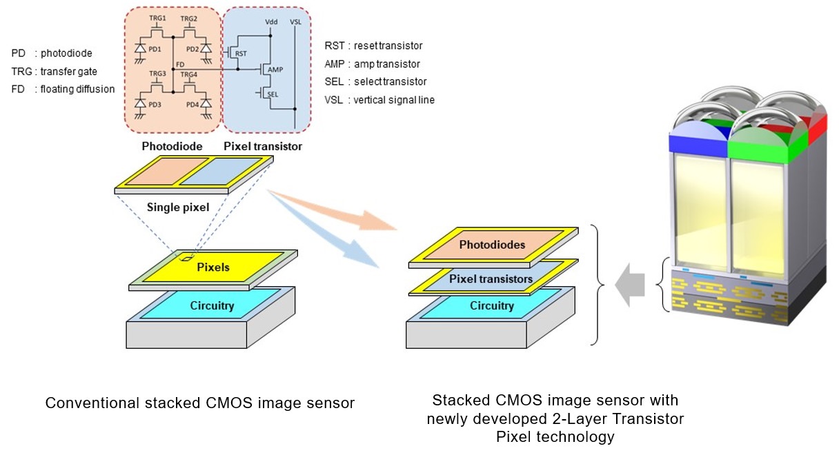
Sony’s Semiconductor division has announced that it successfully developed the world’s first stacked CMOS image sensor technology with two-layer transistor pixels. This new technology separates the photodiodes from the pixel transistors onto different substrate layers, which nearly doubles the amount of light a single pixel can capture compared to more conventional image sensors.
Sony explains that typical image sensors place photodiodes and pixel transistors on the same substrate, but in this new design, it was able to separate them onto different substrate layers. In addition to optimized architectures, Sony says this stacked technology also enables them to increase the size of the amp transistors. These two benefits mean the individual pixels will have nearly double the saturation signal level and will be able to reduce the noise of images captured in a low-light environment.
Sony says that the new stacking technology enables the adoption of architectures that allow the photodiode and pixel transistor layers to each be optimized, thereby approximately doubling saturation signal level relative to conventional image sensors and, in turn, widening dynamic range.
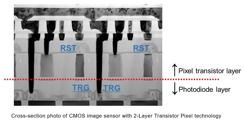
“Additionally, because pixel transistors other than transfer gates (TRG), including reset transistors (RST), select transistors (SEL), and amp transistors (AMP), occupy a photodiode-free layer, the amp transistors can be increased in size,” Sony says. “By increasing amp transistor size, Sony succeeded in substantially reducing the noise to which nighttime and other dark-location images are prone.”
Sony specifically notes that this technology is going to make for increasingly high-quality imaging in the case of smartphone photography. The new technology’s pixel structure will enable pixels to maintain or improve their existing properties at not only current but also smaller pixel sizes.
Sony doesn’t specify when it plans to manufacture sensors at scale using this technology but does say it will continue to iterate on the design to further increase image quality in sensors large and small.
More info on Sony’s website.


